AMD Instinct MI300 Series Architecture Deep Dive Reveal: Advancing AI And HPC
AMD Instinct MI300 Family Architecture Explained: Gunning For Big Gains In AI

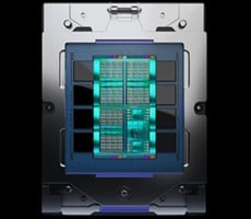
AMD has previously shown off its Instinct MI300A and MI300X accelerators at various events, but today numerous architectural details were revealed. To quickly recap some of the high-level details and bring everyone up to speed, the AMD Instinct MI300A is the company’s first data center APU accelerator for AI and HPC applications that combines its CDNA 3 data center GPU compute architecture with Zen 4 CPU chiplets (24 Genoa cores) and 128GB of shared, unified HBM3 memory, accessible to both the GPU accelerators and CPU cores. The AMD MI300A reportedly delivers 8x higher performance and 5x better efficiency than the prior-gen CDNA 2-based Instinct MI250X accelerator.
The AMD Instinct MI300X is a somewhat different animal. The MI300X eschews the three Zen 4 chiplets (and hence the CPU cores) of the MI300A in favor of two more CDNA 3 XCD (Accelerator Complex Die) chiplets for what is effectively an all-GPU/accelerator design. It also expands the memory capacity to 192GB of HBM3. Both the MI300A and MI300X offer about 5.3TB/s of aggregate memory bandwidth, and massive 17TB/s of peak bandwidth from 256MB of AMD Infinity Cache, and the MI300X is optimized for HPC, LLMs, and associated AI workloads as well.
We’ve covered Zen 4 many times previously, and CDNA 3 at a high-level too. For more detailed Zen 4 information, check out this article – the Zen 4 cores used on the MI300A are unchanged from those used on Genoa-based EPYC server processors. CDNA 3 is the AMD compute accelerator architecture used in the MI300 family. The CDNA 3 chiplets on the MI300A and MI300X will be manufactured on a 5nm process, and unlike the coherent memory architecture of RDNA 3 GPUs, CDNA 3 moves to a unified memory architecture, where the CPU and GPU compute accelerator cores can all access the same memory. For its intended applications, the move to a unified memory architecture should improve efficiency, because it minimizes redundant memory copies by eliminating the need to copy data from one memory pool to the other.
A Closer Look At The AMD Instinct MI300 Family
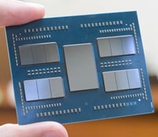
How the CPU (CCD) and GPU/Accelerator (XCD) chiplets are linked across the package and via AMD’s Infinity Fabric is unique to the MI300 family, though.The AMD Instinct MI300A and MI300X are fundamentally similar. At a high-level, the main difference is that the three CCDs used on the MI300A to integrate CPU cores are replaced by two additional XCDs on the MI300X. That means the total chiplet count is different, too. The MI300A is comprised of 13 chiplets (3 x CCD, 6 x XCD, 4 x IO) while the MI300X uses 12 (8 x XCD, 4 x IO). The MI300X also has more HBM3 memory (128GB vs. 192GB). Both have four base IO dies and are built using 3D hybrid bonded SoIC technology and 2.5D silicon interposers, in addition to traditional technologies. The combination of 3D stacking and the use of 2.5D silicon interposers is why AMD says the Instinct MI300 family uses advanced 3.5D packaging.
Tunneling down a little deeper, the AMD Instinct MI300 features a 128-channel interface to its HBM3 memory, with each IO die connected to two stacks of HBM3. The MI300s also feature 256MB of AMD Infinity Cache, and an Infinity Fabric network-on-chip. The Infinity Fabric is comprised of 128 total 32Gb links, 64 of which (4 x 16) are capable of both PCIe Gen 5 and Infinity Fabric, while the remaining 64 (4 x 16) are purely Infinity Fabric.
As noted there are four base IO die chiplets on the MI300. These four chiplets are linked together using a new AMD Infinity Fabric AP (Advanced Package) Interconnect. Due to the different configurations of the MI300A and MI300X—to reiterate, the AMD Instinct MI300A has CPU cores, while the MI300X does not—they can function both as a self-hosted PCIe root complex APU or as a PCI endpoint device. This is an important capability that allows for some design flexibility at the system level.
Each of the Zen 4 CCDs on the MI300A feature 8 CPU cores and 32MB of shared L3 cache, again, just like AMD’s EPYC server processors. The CDNA 3 XCDs are all new, however, and mark the first time AMD has “chipletized” the GPU. AMD wanted to scale beyond what was possible with a monolithic GPU, so they effectively deconstructed a traditional GPU design and re-architected it with chiplets in mind.
Each XCD has 40 CDNA 3 compute units in total, but only 38 are enabled at this time to maximize yield. 4MB of L2 cache is shared by the CUs, and the L1 cache is optimized for bytes/FLOP. Although there are multiple XCDs on the Instinct MI300s, note that they function as a single device. The Infinity Fabric interface between the chiplets enables multi-XCD hardware assisted cache coherence, and they all share access to the same 256MB of on-board, ultra-high-bandwidth Infinity Cache.
The CDNA 3 compute units have also been upgraded in a number of ways over CDNA 2. The CUs now individually support double the low precision matrix ops per clock, and AMD has added 2:4 structured sparsity on the matrix cores as well as support for TF32 (Tensor Flow) and FP8 numerical formats. TF32 allows in-line utilization of FP32 data structures, and ultimately offers higher computational throughput by truncating the mantissa. E5M2 and E4M3 FP8 are both supported for training and inference workloads, and the FP8 implementation is OCP FP8 compliant, though the MX block micro-scaling formats are not supported in this generation.
To further improve utilization and performance, AMD also added co-issue support for enhanced thread-level parallelism versus the previous generation. It can now issue FP32 or Int32 ops with FP32 or FP64 to accelerate address generation in parallel with execution of FP32 or FP64 operations, which allows for higher FP32 throughput by making better utilization of the CUs. There is also a deeper Instruction Buffer, primarily to better feed the co-issue. There can be up to 24 instructions in the buffer, and AMD doubled the L1 instruction and vector cache capacities.
All of the formats supported and their throughput are detailed in the table above. The goals were to focus on AI tensor operations and formats and ensure significantly improved performance over MI200. AMD notes that for both FP16 and FP32, the rates in the table refer to the non-packed vector instructions and highlight the increased throughput that comes as a result of the co-issue enhancements. The FP16, BF16, FP8 and INT8 matrix core throughput results on MI300X refer to dense compute. Throughput for 2:4 structured sparsity is not reflected in this table.
Here is a simplified overview of how the memory subsystems are constructed on the MI300X and MI300A. As mentioned, the design features a 128 channel fine-grained interleaved memory system, with two XCDs (or three CCDs) connected to each IO die, and then two stacks of HBM3. Each stack of HBM is 16 channels, so with two HBM stacks each, that’s 32 channels per IO die. And with 4 IO dies per MI300, the total is 128.
The XCDs or CCDs are organized with 16 channels as well, and they can privately interface with one stack of HBM, which allows for logical spatial partitioning, but we’ll get to that in a bit. The vertical and horizontal colored bars in the diagrams represent the Infinity Fabric network on chip, which allows the XCDs or CCDs to interface within or across the IO dies to access all of the HBM in the system. You can also see where the Infinity Cache sits in the design. The Infinity Cache is a memory-side cache and the peak bandwidth is matched to the peak bandwidth of the XCDs – 17TB/s. In addition to improving effective memory bandwidth, note that the Infinity Cache also optimizes power consumption by minimizing the number of transactions that go all the way out to HBM.
The AMD Instinct MI300s also offer a number or partitioning modes. The MI300A can be configured with a single partition or in three partitions, but with only a single NPS mode, namely NPS1 (NUMA Node Per Socket). The MI300X, however, offers four partition modes, with up to eight GPU partitions to maximize GPU utilization, and two NPS modes -- either NPS1, for a single memory partition or NPS4 for quad memory partitions.
Building The AMD Instinct MI300 Family
AMD also talked a bit about how it actually built the Instinct MI300. The SoIC hybrid bonding technology that AMD first leveraged with 3D V-Cache is used extensively on the MI300, but it has been scaled up significantly. All of the XCDs and CCDs, which are manufactured at 5nm, are stacked onto the base IO dies that are manufactured at 6nm using the same 9µ TSV pitch. The company had to do some significant pre-planning to pull it all off, though.
One of the main goals of designing chiplets is the re-use of IP across multiple designs. Since MI300 is using an existing CCD design, that CCD had to originally be built with multiple future products in mind. As such, the CCD features some on-pad via interfaces that parallel the GMI SerDes stack on the GPU. When AMD’s CPU and GPU teams consulted at the time, luckily there was space in the CCD floor plan to accommodate the necessary links and it required only some minor changes to the top layer of metal.
But, to make everything ultimately fit together, AMD also had to design the base IO dies to connect to each other, the HBM, the CCDs and the XCDs in multiple ways. To do so, AMD essentially mirrored the mask set used to manufacture the IO die and made only minor changes to some circuits. The IO die, CCDs, and XCDs, are then rotated, or mirrored and rotated in the case of some dies, to piece everything together.
Of course, mirroring and rotating dies also required some careful planning for signaling and power delivery. The XCDs and CCDs are only rotated (AMD doesn’t have mirrored mask sets for those chiplets), but AMD still needed to originally design them to work in either configuration from the start.
Power delivery was a particularly tough challenge. Hundreds of amps are delivered to the top compute die through the base IO die. As such, the company had to do a lot of simulation and analysis to understand the power density differences across the chiplets and ensure they not only have enough power, but also that they deliver it without disrupting other parts of the chip while reliably supporting the highest-power modes.
Clearly, the AMD Instinct MI300 family was a monumental engineering feat. Getting 12 or 13 chiplets to function logically as a monolithic piece of silicon while offering high performance and reliability, as well as the flexibility to operate in multiple modes, was ambitious to say the least. AMD seems to have pulled it off, though.
AMD Instinct MI300 Performance Claims
During the Advancing AI event livestream, AMD also disclosed some performance data for the Instinct MI300A and MI300X versus competitive solutions from NVIDIA, which paints a favorable picture...The summary data above shows some spec and tpeak theoretical compute performance comparisons versus the NVIDIA H100. Notably, both the M300A and M300X have significantly more memory capacity and memory bandwidth. Factor in those advantages with the MI300s' peak theoretical compute capabiltiies and it shows the MI300A -- which has fewer XCDs -- effectively matching the H100 in the AI-related metrics, but surpassing the H100 in the HPC workloads. The MI300X theoretically wins across the board.
With a number of popular LLMs and AI inference and training workloads, AMD's data also shows the Instinct MI300X offering a 10% - 60% performance advantage over the H100. In a single server equipped with 8 x MI300X cards, versus an NVIDIA H100 HGX (also with 8 GPUs), AMD shows performance parity training with the 30M parameter MPT foundational model.
AMD is also claiming a 4X performance advantage for the Instinct MI300A versus H100 in the OpenFOAM HPC Motorbike benchmark and 10-20% advantages in various other HPC workloads.
AMD is also claiming a 2X performance per watt advantage for Instinct MI300A over the NVIDIA Grace Hopper GH200 chip. Of course, all of these numbers have to play out in the real world, but we suspect AMD is being forthright with these disclosures.


